


[ad_1]
Among the new semiconductor entrants embody Signature IP, which was based in 2021 to develop superior network-on-chip (NoC). EdgeCortix designs AI-specific processor structure from the bottom up, and M31 Know-how Company is a silicon IP supplier. M31, with a middle in Bengaluru, is concerned in IP improvement, IC design, and digital design automation fields, together with reminiscence compilers and commonplace cell library options.
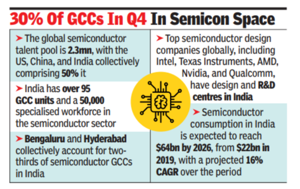
Nasscom-Zinnov acknowledged that the worldwide semiconductor expertise pool is 2.3 million, with the US, China, and India collectively comprising 50% of the worldwide expertise pool.
Bengaluru and Hyderabad collectively account for two-thirds of semiconductor GCCs in India, residence to over two-thirds of the 55 semiconductor GCCs. India has over 95 GCC models and a 50,000 specialised workforce, underlining India’s dedication to the semiconductor sector.
Some key roles throughout the semiconductor worth chain embody ASIC design engineer, reliability take a look at engineer, clear room technician, chip encapsulation specialist, PCB (printed circuit board) design engineer, RF take a look at engineer, and skinny movie engineer.
The Nasscom-Zinnov report stated that the GCCs are remodeling their India facilities into transformation hubs, engaged on the designing and improvement of chips, with fabrication outsourced to specialised foundries. Micron’s India middle has lined up a 1 TB 232-Layer 3D TLC NAND Flash reminiscence chip for numerous purposes in enterprise, client, and gaming. Micron has lined up a $2.7 billion funding for its semiconductor chip meeting and take a look at facility in Sanand.
The highest cdhip design corporations globally, together with Intel, Texas Devices, AMD, Nvidia, and Qualcomm, have design and R&D facilities in India. Just lately, AMD inaugurated its largest world design middle in Bengaluru, planning to make use of round 3,000 engineers within the coming years. The AMD Technostar campus is a part of the corporate’s $400 million funding in India over the subsequent 5 years. The campus will function a middle of excellence throughout high-performance CPUs for the information middle and PCs, information middle and gaming GPUs, and adaptive SoCs and FPGAs for embedded gadgets.
[ad_2]
2024-04-05 21:34:06
[


+ There are no comments
Add yours